OhmPediaSemiconductor DevicesBipolar Junction Transistor
Bipolar Junction Transistor
双极结型晶体管 I_C = β · I_B
- Symbol
- I_C = β · I_B
- Unit
- β (h_FE) dimensionless, typically 50–500 · V_BE ≈ 0.65 V · V_CE(sat) ≈ 0.1–0.3 V
- Section
- Semiconductor Devices
- Published
- 2026-09-03
- Author
In a BJT the base-emitter junction is forward biased and the base-collector junction reverse biased; electrons injected into the thin base region are swept into the collector. The result is I_C = β · I_B over a wide range, with β set by the doping and geometry rather than by the user.
A three-terminal current-controlled device in which a small base current regulates a much larger collector current.
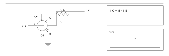
Three regions, three jobs
Cut-off, active and saturation are not device states but bias conditions, and each has a use. Cut-off is the off switch. Saturation is the on switch, where both junctions are forward biased and the collector-emitter voltage collapses to 0.1–0.3 V. The active region is where the transistor amplifies and where β applies.
- Cut-off: V_BE < 0.5 V, I_C ≈ leakage. Used as an open switch.
- Active: V_BE ≈ 0.65 V, I_C = βI_B. Used for amplification and current sources.
- Saturation: I_B > I_C/β, V_CE ≈ 0.1–0.3 V. Used as a closed switch.
β is a rumour, not a specification
Datasheets give a minimum, a typical and a maximum for h_FE, and for a 2N3904 those are 100, 200 and 300 at 10 mA — and the spread widens with temperature and current. Any design whose bias point depends on the exact value of β is not a design. The standard fix is emitter degeneration: an emitter resistor makes the bias depend on resistor ratios, which are controlled, rather than on β, which is not.
The four rules of thumb
For a silicon NPN in the active region, almost every hand calculation starts from four approximations.
| Quantity | Approximation | When it is safe |
|---|---|---|
| V_BE | 0.65 V (0.7 V at higher current) | Any active-region bias calculation |
| V_CE(sat) | 0.1 V small signal, 0.2–0.3 V at 100 mA+ | Switch design and saturation headroom |
| β | Take the datasheet minimum, not typical | Always, for worst-case design |
| r_e (intrinsic emitter resistance) | 26 mV / I_C(mA) ≈ 26 Ω at 1 mA | Gain and input-impedance estimates |
Heat and the thermal spiral
V_BE falls about 2 mV/K while leakage roughly doubles every 10 K. At fixed base drive, both effects raise the collector current as the junction heats, which raises the dissipation, which raises the temperature further. Emitter resistance and a heat-sinked package are the two standard defences; without them, power transistors in parallel share current unequally and one device takes the whole load.
An NPN drives a 5 V relay coil of 120 Ω from a 3.3 V logic output. Coil current is 5/120 = 41.7 mA. With the datasheet minimum h_FE of 100, the base needs at least 0.42 mA; using a 5× overdrive factor for hard saturation gives 2.1 mA. The base resistor is (3.3 − 0.7)/0.0021 = 1.24 kΩ, so 1.2 kΩ is chosen. The transistor dissipates 41.7 mA × 0.25 V = 10.4 mW in saturation — nothing. The same relay driven from the collector without the base resistor would instead dissipate 41.7 mA × 5 V = 209 mW and destroy the part.
Read first
- Diode 二极管
Adjacent entries
- MOSFET 金属氧化物半导体场效应管
Off the shelf
Sources
- University of Mississippi http://www.phy.olemiss.edu/~cremaldi/PHYS417/DiodeBasics.pdf
- Northern Illinois University https://nicadd.niu.edu/~fortner/course/phys375/lect/p375_05a.pdf
- Physics LibreTexts https://phys.libretexts.org/Bookshelves/University_Physics/University_Physics_(OpenStax)/University_Physics_II_-_Thermodynamics_Electricity_and_Magnetism_(OpenStax)