OhmPediaSemiconductor DevicesMOSFET
MOSFET
金属氧化物半导体场效应管 I_D = ½ k (V_GS − V_th)²
- Symbol
- I_D = ½ k (V_GS − V_th)²
- Unit
- V_th in volts (1–4 V typical) · k in A/V² · R_DS(on) in milliohms
- Section
- Semiconductor Devices
- Published
- 2026-09-15
- Author
In an enhancement-mode MOSFET a gate voltage above the threshold inverts the semiconductor surface under the gate, forming a conducting channel. No steady gate current flows because the gate is insulated, so the device is controlled by voltage rather than by current, and its on-state is characterised by a resistance rather than by a saturation voltage.
A voltage-controlled transistor in which an insulated gate sets how much current flows between drain and source.
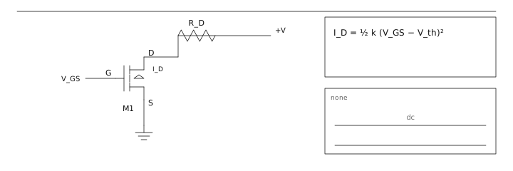
Threshold, overdrive and the square law
Below threshold the device is off apart from sub-threshold leakage. Above it, drain current rises approximately with the square of the gate overdrive, I_D ≈ ½k(V_GS − V_th)². Driving a logic-level FET with 3.3 V when its threshold is 3 V leaves 0.3 V of overdrive and a channel barely able to conduct; the same part with 10 V of gate drive is a fraction of an ohm. Gate drive voltage, not the headline current rating, is what most often makes a MOSFET circuit fail.
R_DS(on) and the temperature surprise
The on-state resistance is quoted at 25 °C and roughly doubles by 125 °C for silicon, because carrier mobility falls with temperature. A 10 mΩ FET used at 20 A dissipates 4 W cold and 8 W hot — and that positive temperature coefficient is a gift: paralleled MOSFETs share current automatically, unlike BJTs.
| R_DS(on) at 25 °C | Typical at 125 °C | 20 A dissipation cold | 20 A dissipation hot |
|---|---|---|---|
| 5 mΩ | ≈ 9 mΩ | 2.0 W | 3.6 W |
| 10 mΩ | ≈ 19 mΩ | 4.0 W | 7.6 W |
| 40 mΩ | ≈ 75 mΩ | 16 W | 30 W |
Gate charge is the real switching limit
Because the gate is a capacitor, driving it consumes energy at every edge: P = Q_g · V_GS · f_sw. A part with 30 nC of total gate charge driven to 10 V at 200 kHz burns 60 mW in the driver alone, before any conduction loss. Total gate charge, not gate capacitance, is the number to quote, because it also accounts for the Miller plateau that keeps the gate voltage stuck while the drain voltage swings.
Body diode, avalanche and dead time
Every MOSFET contains a parasitic diode from source to drain. It clamps inductive kicks in low-side switching, which is convenient, but it is slow and its reverse recovery adds loss. In a synchronous half-bridge both FETs must be off long enough between transitions — dead time — that the two never conduct simultaneously, because a shoot-through current is limited only by the two channels and destroys both devices within microseconds.
A low-side N-channel MOSFET switches a 12 V, 5 A load with R_DS(on) = 10 mΩ at 25 °C. Conduction loss is 25 × 0.010 = 0.25 W cold. At 100 °C the resistance is about 16 mΩ, giving 0.40 W, and with a 50 K/W junction-to-ambient path the junction runs 20 K above ambient — acceptable without a heatsink. Now drive the same FET from a 3.3 V logic pin through a 100 Ω gate resistor: the RC of 100 Ω and 2 nF of gate capacitance gives a 200 ns rise, and during each transition the FET passes through a region where it drops 6 V at 2.5 A — an average of 7.5 W for 200 ns, twice per switching cycle.
Read first
- Diode 二极管
Adjacent entries
- Bipolar Junction Transistor 双极结型晶体管
Off the shelf
Sources
- Northern Illinois University https://nicadd.niu.edu/~fortner/course/phys375/lect/p375_05a.pdf
- University of Mississippi http://www.phy.olemiss.edu/~cremaldi/PHYS417/DiodeBasics.pdf
- Physics LibreTexts https://phys.libretexts.org/Bookshelves/University_Physics/University_Physics_(OpenStax)/University_Physics_II_-_Thermodynamics_Electricity_and_Magnetism_(OpenStax)