OhmPediaDigital LogicLogic Gate
Logic Gate
逻辑门 Y = f(A, B, …)
- Symbol
- Y = f(A, B, …)
- Unit
- logic 0 / 1 · V_IL, V_IH in volts · t_pd in nanoseconds
- Section
- Digital Logic
- Published
- 2026-08-25
- Author
A logic gate implements one of the Boolean operations — AND, OR, NOT, NAND, NOR, XOR — with an output that is always a valid logic level regardless of how degraded the input was. That restoration, not the logic function, is what makes gates useful: they can be cascaded indefinitely without accumulating noise.
A circuit that computes one Boolean function of its inputs and restores the result to a valid logic level.
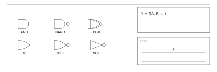
The six gates and their universality
NAND alone, or NOR alone, can implement any Boolean function, which is why they are the gates that integrated circuits actually build. AND and OR are made by inverting the output of a NAND or NOR, and XOR needs four NANDs in the classic arrangement — although in CMOS it is normally built directly because the transistor count of the NAND version is far higher.
| Gate | Output is 1 when | CMOS transistors | Functionally complete alone |
|---|---|---|---|
| NOT | input is 0 | 2 | No |
| NAND | not both inputs are 1 | 4 | Yes |
| NOR | neither input is 1 | 4 | Yes |
| AND | both inputs are 1 | 6 | No |
| OR | either input is 1 | 6 | No |
| XOR | the inputs differ | 8–12 | No (with constant 1, yes) |
Levels, margins and noise
Datasheets specify V_IH (minimum voltage read as 1), V_IL (maximum voltage read as 0), V_OH (minimum voltage output as 1) and V_OL (maximum output as 0). The noise margin is the gap between them: V_OH − V_IH for a high, V_IL − V_OL for a low. A 74HC gate at 5 V has about 2.5 V of high-level margin, which is why logic survives wiring that would ruin an analogue signal. The margin collapses if you mix families — a 3.3 V output driving a 5 V CMOS input has close to zero margin and will work in one board and not the next.
Propagation delay and fan-out
Each gate adds a delay, and the delay grows with the load capacitance: t_pd ≈ 0.35 R_out C_load for a first-order output. A gate driving 50 pF instead of the datasheet's 15 pF is slower by roughly 3.3×. Fan-out is the number of inputs one output can drive while staying within its DC current rating, but in CMOS the practical limit is almost always capacitive rather than DC.
Unused inputs are not optional
A floating CMOS input sits at an undefined voltage, and both transistors of the input inverter may conduct, drawing supply current and injecting noise into the gate. Every unused input must be tied to a supply rail or to another used input. On a board with a 74HC00 quad NAND, leaving three gates unconnected can add tens of milliamps of quiescent current that no schematic shows.
A designer needs an enable that is active only when a write signal is high and a chip select is low. Using a 74HC00 quad NAND: tie the two inputs of a NAND together to make an inverter, invert the chip select, then NAND the inverted select with write, then invert the result — four gates, all from one package. The alternative is a discrete transistor network plus two pull-up resistors, which is slower and drifts with temperature. Measuring the finished path gives 4 × 9 ns = 36 ns of delay at 15 pF per stage load, plus 25 ns of extra delay from the 50 pF probe capacitance on the final output, for 61 ns total.
Read first
- Boolean Algebra 布尔代数
Adjacent entries
- Boolean Algebra 布尔代数
Off the shelf
Sources
- Northern Illinois University https://nicadd.niu.edu/~fortner/course/phys375/lect/p375_05a.pdf
- Physics LibreTexts https://phys.libretexts.org/Bookshelves/University_Physics/University_Physics_(OpenStax)/University_Physics_II_-_Thermodynamics_Electricity_and_Magnetism_(OpenStax)
- NIST https://www.nist.gov/pml/owm/si-units-electric-current